This system can realize the efficient and automatic testing of copper clad ceramic plate, and the system can be embedded in the customer’s automated product line to help customers achieve strict product quality control.At the same time, this system can also be used for other semiconductor devices and package testing, such as discrete devices, optoelectronic devices and IGBT power module products.
Performance
Features
- Automated assembly line inspection
Implemented automatic loading and unloading,automatic detection, intelligent evaluation, sorting after drying, etc.
- Intelligent defect evaluation
Intelligent identification and statistics of defect size,area, and quantity information, providing data support for product qualification.
- Automatic calibration of each channel
Ensure uniform and realistic imaging.
- Full coverage detection
Avoiding missed defects.
- Automatic water circulation
It can ensure automatic pumping and adding water to a fixed height before each detection; Reduce the impact of water level and buoyancy on equipment detection accuracy.
System Composition
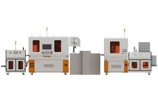
The whole system consists of high-precision mechanical and electrical system, ultrasonic automatic inspection and intelligent evaluation system, drying and automatic sorting system. Among them, the electrical of the automatic mechanical platform is composed of feeding device, automatic plate flap mechanism, two-dimensional code scanning device, material transfer device, detection sink, transmission device,main frame, motion control system and supporting module, dry plate combination device and cutting sorting device. The phased array ultrasonic testing system mainly includes ultrasonic phased array board, high-end customized phased array probe and wedge, intelligent detection and automatic evaluation software.
Technical Specifications
- System repeatability: ± 0.03mm
- Maximum scanning speed: 500mm/s
- Detection imaging resolution: 0.2×0.2mm
- System detection frequency: 20MHz or more
- Three-axis module travel: can be customized according to customer needs
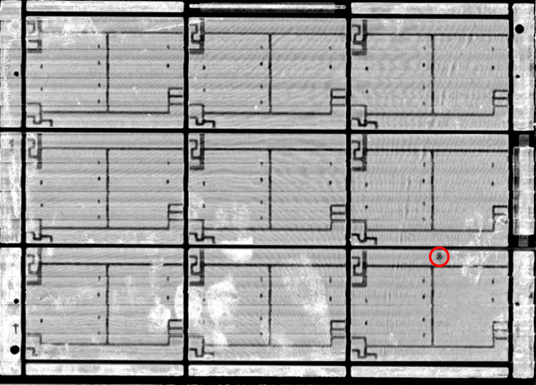
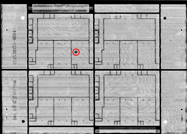
Typical Detection Map


